-
Two capacitors are connected in parallel through a switch. C1= 1uF, C2=
0.25uF.
Initially the switch is open, C1 is charged to 10V. What happens if we close the switch? No losses in wires and capacitors.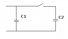
Answers & follow ups
-
You have 2 switches to control the light in the long corridor.
You want to be able to turn the light on
entering the corridor and turn it off at the other end. Do the wiring circuit.
Answers & follow ups
-
There are 3 switches that can turn on and off a light in the room.
How to connect them?
Answers & follow ups
-
What will be the voltage level between the two capacitors? The Vcc = 10v DC.
Sent by Tanh, VLSI engineer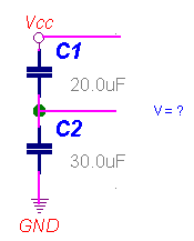 Answers & follow ups
-
Suppose, you work on a specification for a system with some digital parameters.
The spec table has has Min,Typ and Max colomns for each parameter. In what column would you put
a Setup time and a Hold time?
Answers & follow ups
-
Design a simple circuit based on combinational logic to double the
output frequency.
Answers & follow ups
-
8bit ADC with parallel output converts an input signal into digital numbers. You have
to come up with an idea of a circuit , that finds MAX of every
10 numbers at the output of the ADC.
Answers & follow ups
-
Implement a comparator that compares two 2-bit numbers A and B. The comparator should have 3 outputs:
A > B, A < B, A = B. Do it two ways:
- using combinational logic;
- using multiplexers. Write HDL code for your schematic at RTL and gate level.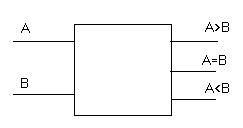
Answers & follow ups
-
You have a 8 bit ADC clocking data out every 1mS. Design a system that
will sort the output data and keep the statistics of how often
each binary number appears at the output of ADC.
Answers & follow ups
-
What types of flip-flops do you know?
Answers & follow ups
-
Implement D- latch from
- RS flip flop;
- multiplexer.Answers & follow ups
-
How to convert D-latch into JK-latch and JK-latch into D-latch?
Answers & follow ups
-
There are two counters to 16, built from negedge D- FF .
The first circuit is synchronous and the second one is "ripple" (cascading).
Which circuit has less propagation delay?
Answers & follow ups
-
What is the difference between a flip-flop and a latch?
Write an HDL code for their behavioral models.Hint from Hitequest
-
Describe the operation of a DAC. What are the most important parameters of a
DAC? Do we really need both INL and DNL to estimate linearity?
Hint from Hitequest
-
Compare briefly all types of ADC that you know .
Hint from Hitequest
-
How will the output signal of an ideal integrator look like after
- a positive pulse is applied to the input;
- a series of 10 positive pulses ?Hint from Hitequest
-
How to design a divide-by-3 counter with equal duty cycle ?
question from AnonymousAnswers & follow ups
-
For an 8-bit flash A/D converter with an input range from 0V to 2.55V, describe what happens when the input voltage
changes from 1.27V to 1.28V
Answers & follow ups
-
Your system has CPU, ALU and two 8bit registers. There is no external memory.
Can you swap the contence of the registers ?
Answers & follow ups
-
We swapped 2 transistors in CMOS inverter (put n-transistor at the top and p-transistor
at the bottom).
Can this circuit work as a non-inverting buffer?
(By E.Martovetsky,design eng)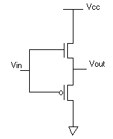
NO, IT CAN NOT! - Discussion with SriramYES, IT CAN! - Discussion with PeterYuri M., National Semi, PHD
-
Convert D-latch into divider by 2.
What is the max clock frequency the circuit can handle ?
T_setup= 6nS
T_hold = 2nS
T_propagation = 10nSHint from Hitequest
-
The circle can rotate clockwise and back. Use minimum hardware to build
a circuit to indicate the direction of rotating.
 Hint from Hitequest
-
Provide 2-dimentional plot of how the output of digital circuit will look like, if on axis X we sweep the clock period, while on axis Y we sweep the data setup time (Tclk vs Tsetup).
-
For chip design/test/product engineers :
An IC device draws higher current when temperature gets:
- higher?
- lower?Hint from Hitequest
-
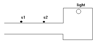
To enter the office people have to pass through the corridor. Once someone
gets into the office the light turns on. It goes off when noone is present in the
room. There are two registration sensors in the corridor. Build a state
machine diagram and design a circuit to control the light.
-
A voltage source with internal impedance Z_source = 50 OHm is connected to a transmission line
with Z = 50 OHm. Z_load is also 50 OHm.
The voltage source generates a single voltage step 1V.
What will be the voltage level on the load:
a) 2V , because the reflected signal will be in-phase with the incident signal;
b) 0.33V , because the voltage is devided between Z_source , Z_load and Z_transm.line;
c) 0.5V , because the voltage is devided between Z_source and Z_load.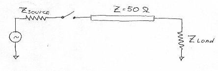
Hint from Hitequest
-
Draw a transistor schematic of NOR gate,it's layout and a cross section of the layout.
This question is quite popular on interviews.
-
The silicon of a new device has memory leak. When all "0" are written into RAM, it reads back all "0" whithout
any problem. When all "1" are written, only 80% of memory cells are read back correctly.
What can be possibly the problem with the RAM?
M.Altshuler, product engineer.
-
Draw a CMOS inverter. Why does CMOS technology dominate in VLSI manufacturing?
L.Backer, DFT engineer
-
Design a FIFO 1 byte wide and 13 words deep. The FIFO is interfacing 2 blocks with different clocks.
On the rising edge of clk the FIFO stores data and increments wptr.
On the rising edge of clkb the data is put on the b-output,the rptr
points to the next data to be read.
If the FIFO is empty, the b-output data is not valid. When the FIFO is full the existing data should not be overriden.
When rst_N is asserted, the FIFO pointers are asynchronously reset. module fifo1 (full,empty,clk,clkb,ain,bout,rst_N)
output [7:0] bout;
input [7:0] ain;
input clk,clkb,rst_N;
output empty, full;
reg [3:0] wptr, rptr;
...
endmodule
Hint from Hitequest
-
What does CMOS stand for? VLSI? ASIC?
This was in the series of quick questions in the interview at Analog Devices. We use these abbreviations daily, but not everyone remembers what they stand for.Hint from Hitequest
-
Design a COMBINATIONAL circuit that can divide the
clock frequency by 2.
Answers & follow ups
- Design a 2bit up/down counter with clear using gates. (No verilog or
vhdl)
- We have a circular wheel with half painted black and the other half
painted white. There are 2 censors mounted 45 degree apart at the
surface of this wheel( not touching the wheel) which give a "1" for
black and "0" for white passing under them. Design a circuit to detect
which way the wheel is moving. Can not assume any fixed position for
start.
- We have a FIFO which clocks data in at 100mhz and clocks data out at
80mhz. On the input there are only 80 data bits in any order during each 100
clocks. In other words, a 100 input clock will carry only 80 data bits, and
the other twenty clocks carry no data (data is scattered in any order).
How big the FIFO needs to be to avoid data over/under-run.
Follow Ups
- Instead of specifying SETUP and HOLD time, can we just specify a SETUP time for '1' and a SETUP time for '0'?
Follow ups
- Here some hardware digital design specific questions, offered by Suhas:
(1) When will you use a latch and a flipflop in a sequential design?
(2) Design a 1-bit fulladder using a decoder and 2 "or" gates?
(3) You have a circuit operating at 20 MHz and 5 volt supply. What would you do to reduce the power consumption in the circuit- reduce the operating frequency of 20Mhz or reduce the power supply of 5Volts and why?
(4) In a nmos transistor, how does the current flows from drain to source in saturation region when the channel is pinched off?
(5) In a SRAM circuit, how do you design the precharge and how do you size it?
(6) In a PLL, what elements(like XOR gates or Flipflops) can be used to design the phase detector?
(7) While synthesis of a design using synopsys design compiler, why do you specify input and output delays?
(8) What difference do you see in the timing reports for a propogated clock and an ideal clock?
(9) What is timeborrowing related to Static timing anaylsis in Primetime?
-
What is the purpose of a diode next to relay on schematics?
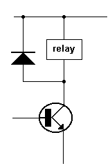
Answers & follow ups
- Design a combinational circuit, that multiplies an input
decimal digit represented in BCD by 5. The output is to be
represented in BCD. Show that the outputs can be obtained
from the input lines without using any logic gates.
-
I got this question on the interview to the company that makes flash memory controllers.
They let me take it home and think for a few days. A.M.
There is a system with 4 flash memory banks. When data comes to the system, it will be randomly sent to one of the 4 banks. The system has a feature called Native Command Queuing (NCQ) which allows the host to send multiple commands at a time.
The number of commands sent at a time is called the queue depth. With a queue depth of 1, only 1 of 4 memory banks will be active.
With a queue depth of 2, we expect 2 of 4 flash memory banks to be active except in the case when both commands are to the same bank.
The question is, what is the expected number of flash memory banks that would be active, given queue depths of:
2, 4, 8, and 16 ?Answers & follow ups
Saturday, 4 February 2012
Electronics Hardware Questions
Subscribe to:
Post Comments (Atom)
MGM Grand Las Vegas Casino Hotel Deals - MapYRO
ReplyDeleteMGM Grand Las Vegas 남양주 출장샵 Casino Hotel Deals & Reviews. Find your way 안산 출장마사지 around the casino, find where everything is 남원 출장마사지 located with 의왕 출장샵 these helpful 광양 출장안마 customer