This blog also belongs to vlsiupdatez.blogspot.com
Saturday, 4 February 2012
VLSI SEMINAR TOPICS
Thanks to visit this blog... if u need any of the below seminar topics plz mail me bsnspkumar_484@yahoo.co.in
- A Smart-Grid Simulator retargeting VCSVMM technology
- ALGORITHMIC GRAPH THEORY
- AN EFFICIENT METHODOLOGY FOR ACHIEVING OPTIMAL POWER AND SPEED IN ASIC
- Analog to Digital Converter in Wireless Local Area Network
- ARITHMETIC CIRCUITS
- bandgap references
- Clock Dividers Made Easy
- Clocking in digital systems
- cmos inverter
- Design And Fast Implementation Of G726 ADPCM Codec for Audio And Speech Applications
- Development of CPLD based memory controller for MPC 603E PPC based single board computer
- FAULTS IN DIGITAL TESTING SYSTEMS
- finfet ppt
- HAZARD AND GLITCHES
- Image Enhancement in the Spatial Domain1
- Image Enhancement in the Spatial Domain2
- Layout Compaction
- MULTI CHIP MODULE1
- NOISE
- perl, a hardware language
- Clocking in digital systems
- STATIC CMOS
- Technology of rocket
- VHDL & DIGITAL CIRCUIT DESIGN
Need of Textbooks softcopies
PG text books
if u need soft copy of the textbooks mentioned below can mail me bsnspkumar_484@yahoo.co.in
B.Tech textbooks
- Rabaey_-_Digital_Integrated_Circuits_-_A_Design_Perspective
- Kumar, Digital Signal Processing Laboratory, (CRC 2005)
- Computer Architecture Patterson Hennessy Solutions case_solutions
- Design of Analog CMOS Integrated Circuits (Behzad Razavi)marcado
- J.L.Hennessy, D.A.Patterson - Computer Architecture. A Quantitative Approach. 3rd Edition
- rf_microelectronics__behzad_razavi_
- Verilog.Digital.Design.Synthesis by salmir palnitkar
- Wiley,.Verilog.Coding.for.Logic.Synthesis.(2003).Spy
- wiley_-_statistical_digital_signal_processing_and_modeling
B.Tech textbooks
- The_C_programming_Language_-_Dennis_Ritchie
- The C++ Programming Language 3rd.Ed 1997
- Adobe_Photoshop_-_Every_Tool_Explained
- Visual_Studio_C#_Web_Developers_Guide
- matlab_primer_-_sigmon___davis__crc_press_2002_
- Addison_Wesley_-_Embedded_C
- Engineering_Mathematics_4E
- Java_Complete_Refference
- McGraw_Hill_-_Digital_Communications_By_John_Proakis_4th_Edition
- _Sybex_-_CCNA_2.0_Study_Guide_(640-507)
- 06-VLSI-design-styles
- All_Circuits_for_the_Hobbyist
- Applied_Mathematics_for_Engineers
- Automatic_Control_Kuo_Sol
- Ayala - The 8051 Microcontroller
- Communication_Systems-_Simon_Haykin_4th_Edition
- CommunSyst_muya
- Digital_Communication_Systems-_Peyton_Z._Peebles_Jr.
- Digital_Design_Principles_and_Practices-_John_F._Wakerly,_3rd_Edition
- Electromagnetics-_William_H._Hayt_Jr.,_John_A._Buck,_6th_Edition,_Mcgraw_Hill
- Integrated_Electronics
- morris_mano
- Sadiku_-_Elements_of_electromagnetics
- Schaums.Outlines.of.Digital.Signal.Processing
- Schaum's.Outline.of.Electronic.Devices.and.Circuits
- Schaum's_Outline_of_Electromagnetics
- Signals_And_Systems
- Solutions_to__Engineering_Electromagnetics_-_Hayt_-_6th_edition
- The_Illustrated_Dictionary_of_Electronics
Digital questions -6
| 26. | What is the major advantage of the J-K flip-flop over the S-R flip-flop? | |||||||
|
| 27. | Decoupling capacitors should be tied from VCC on one device to ground on a different device. | |||
|
| 28. | One example for the use of a Schmitt trigger is as a(n): | |||||||
|
Digital questions-5
| 21. | What is the difference between setup time and hold time? | |||||
|
| 22. | Define a race condition for a flip-flop. | |||||
|
| 23. | Which of the following flip-flop timing parameters indicates the time it takes a Q output to respond to a Cp input? | |||||||
|
| 25. | Why should a LED be pulled LOW from a logic gate rather than pulled HIGH? | |||||||
|
Digital questions - 4
| 16. | A settable flip-flop's normal starting state when power is first applied to a circuit is always the ________ state. | |||||||
|
| 17. | In the automatic reset circuit for a flip-flop, how long does it take the capacitor to completely charge? | |||||||
|
| 18. | The output of a standard TTL NAND gate is used to pull an LED indicator LOW. The LED is in series with a 470- resistor. What is the current in the circuit when the LED is on? resistor. What is the current in the circuit when the LED is on? |
|||||||
|
| 19. | When the inputs to a flip-flop are changing at the same time that the active trigger edge of the input clock is making its transition, this condition is called: | |||||||
|
| 20. | Is the propagation delay from the clock to the output for the 7476 the same as the delay from the set or reset to the output? | |||
|
Digital questions -3
| 11. | What would be the output voltage of a 7814 voltage regulator? | |||||||
|
| 12. | The purpose of a pull-up resistor is to keep a terminal at a ________ level when it would normally be at a ________ level. | |||||||
|
| 13. | Setup time specifies: | |||||||
|
| 14. | Can the automatic RC circuit be used to set a flip-flop rather than reset the flip-flop? | |||
|
| 15. | A Schmitt trigger: | |||||||
|
Digital questions-2
A 0.01- F capacitor is recommended by TTL manufacturers for ________ the power supply. F capacitor is recommended by TTL manufacturers for ________ the power supply. |
||||||||
|
| 7. | Why does the data sheet for the 7476 only give a minimum value for the clock pulse width (both HIGH and LOW)? | |||||
|
| 8. | Why is the Schmitt trigger needed in the 60-Hz TTL-level clock pulse generator? | |||||||
|
| 9. | The main concern when using a pull-down resistor is: | |||||||
|
| 10. | Look up the propagation delay from the clock to the output for the 7476. Are the HIGH-to-LOW and LOW-to-HIGH propagation delays the same? | |||||||
|
Digital questions -1
| 1. | The ________ circuit overcomes the problem of switching caused by jitter on the inputs. | |||||||
|
| 2. | Why would a delay gate be needed for a digital circuit? | |||||||
|
| 3. | An optocoupler is an integrated circuit with an LED and a zener diode encased in the same package. | |||
|
| 4. | A Schmitt trigger has VT+ = 2.0 V and VT– = 1.2 V. What is the hysteresis voltage of the Schmitt trigger? | |||||||
|
| 5. | Which of the following circuit parameters would be most likely to limit the maximum operating frequency of a flip-flop? | |||||||
|
Electronics Hardware Questions
-
Two capacitors are connected in parallel through a switch. C1= 1uF, C2=
0.25uF.
Initially the switch is open, C1 is charged to 10V. What happens if we close the switch? No losses in wires and capacitors.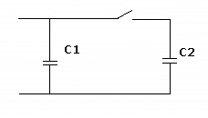
Answers & follow ups
-
You have 2 switches to control the light in the long corridor.
You want to be able to turn the light on
entering the corridor and turn it off at the other end. Do the wiring circuit.
Answers & follow ups
-
There are 3 switches that can turn on and off a light in the room.
How to connect them?
Answers & follow ups
-
What will be the voltage level between the two capacitors? The Vcc = 10v DC.
Sent by Tanh, VLSI engineer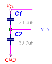 Answers & follow ups
-
Suppose, you work on a specification for a system with some digital parameters.
The spec table has has Min,Typ and Max colomns for each parameter. In what column would you put
a Setup time and a Hold time?
Answers & follow ups
-
Design a simple circuit based on combinational logic to double the
output frequency.
Answers & follow ups
-
8bit ADC with parallel output converts an input signal into digital numbers. You have
to come up with an idea of a circuit , that finds MAX of every
10 numbers at the output of the ADC.
Answers & follow ups
-
Implement a comparator that compares two 2-bit numbers A and B. The comparator should have 3 outputs:
A > B, A < B, A = B. Do it two ways:
- using combinational logic;
- using multiplexers. Write HDL code for your schematic at RTL and gate level.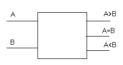
Answers & follow ups
-
You have a 8 bit ADC clocking data out every 1mS. Design a system that
will sort the output data and keep the statistics of how often
each binary number appears at the output of ADC.
Answers & follow ups
-
What types of flip-flops do you know?
Answers & follow ups
-
Implement D- latch from
- RS flip flop;
- multiplexer.Answers & follow ups
-
How to convert D-latch into JK-latch and JK-latch into D-latch?
Answers & follow ups
-
There are two counters to 16, built from negedge D- FF .
The first circuit is synchronous and the second one is "ripple" (cascading).
Which circuit has less propagation delay?
Answers & follow ups
-
What is the difference between a flip-flop and a latch?
Write an HDL code for their behavioral models.Hint from Hitequest
-
Describe the operation of a DAC. What are the most important parameters of a
DAC? Do we really need both INL and DNL to estimate linearity?
Hint from Hitequest
-
Compare briefly all types of ADC that you know .
Hint from Hitequest
-
How will the output signal of an ideal integrator look like after
- a positive pulse is applied to the input;
- a series of 10 positive pulses ?Hint from Hitequest
-
How to design a divide-by-3 counter with equal duty cycle ?
question from AnonymousAnswers & follow ups
-
For an 8-bit flash A/D converter with an input range from 0V to 2.55V, describe what happens when the input voltage
changes from 1.27V to 1.28V
Answers & follow ups
-
Your system has CPU, ALU and two 8bit registers. There is no external memory.
Can you swap the contence of the registers ?
Answers & follow ups
-
We swapped 2 transistors in CMOS inverter (put n-transistor at the top and p-transistor
at the bottom).
Can this circuit work as a non-inverting buffer?
(By E.Martovetsky,design eng)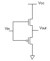
NO, IT CAN NOT! - Discussion with SriramYES, IT CAN! - Discussion with PeterYuri M., National Semi, PHD
-
Convert D-latch into divider by 2.
What is the max clock frequency the circuit can handle ?
T_setup= 6nS
T_hold = 2nS
T_propagation = 10nSHint from Hitequest
-
The circle can rotate clockwise and back. Use minimum hardware to build
a circuit to indicate the direction of rotating.
 Hint from Hitequest
-
Provide 2-dimentional plot of how the output of digital circuit will look like, if on axis X we sweep the clock period, while on axis Y we sweep the data setup time (Tclk vs Tsetup).
-
For chip design/test/product engineers :
An IC device draws higher current when temperature gets:
- higher?
- lower?Hint from Hitequest
-
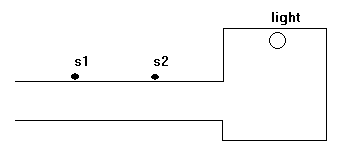
To enter the office people have to pass through the corridor. Once someone
gets into the office the light turns on. It goes off when noone is present in the
room. There are two registration sensors in the corridor. Build a state
machine diagram and design a circuit to control the light.
-
A voltage source with internal impedance Z_source = 50 OHm is connected to a transmission line
with Z = 50 OHm. Z_load is also 50 OHm.
The voltage source generates a single voltage step 1V.
What will be the voltage level on the load:
a) 2V , because the reflected signal will be in-phase with the incident signal;
b) 0.33V , because the voltage is devided between Z_source , Z_load and Z_transm.line;
c) 0.5V , because the voltage is devided between Z_source and Z_load.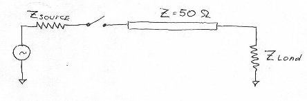
Hint from Hitequest
-
Draw a transistor schematic of NOR gate,it's layout and a cross section of the layout.
This question is quite popular on interviews.
-
The silicon of a new device has memory leak. When all "0" are written into RAM, it reads back all "0" whithout
any problem. When all "1" are written, only 80% of memory cells are read back correctly.
What can be possibly the problem with the RAM?
M.Altshuler, product engineer.
-
Draw a CMOS inverter. Why does CMOS technology dominate in VLSI manufacturing?
L.Backer, DFT engineer
-
Design a FIFO 1 byte wide and 13 words deep. The FIFO is interfacing 2 blocks with different clocks.
On the rising edge of clk the FIFO stores data and increments wptr.
On the rising edge of clkb the data is put on the b-output,the rptr
points to the next data to be read.
If the FIFO is empty, the b-output data is not valid. When the FIFO is full the existing data should not be overriden.
When rst_N is asserted, the FIFO pointers are asynchronously reset. module fifo1 (full,empty,clk,clkb,ain,bout,rst_N)
output [7:0] bout;
input [7:0] ain;
input clk,clkb,rst_N;
output empty, full;
reg [3:0] wptr, rptr;
...
endmodule
Hint from Hitequest
-
What does CMOS stand for? VLSI? ASIC?
This was in the series of quick questions in the interview at Analog Devices. We use these abbreviations daily, but not everyone remembers what they stand for.Hint from Hitequest
-
Design a COMBINATIONAL circuit that can divide the
clock frequency by 2.
Answers & follow ups
- Design a 2bit up/down counter with clear using gates. (No verilog or
vhdl)
- We have a circular wheel with half painted black and the other half
painted white. There are 2 censors mounted 45 degree apart at the
surface of this wheel( not touching the wheel) which give a "1" for
black and "0" for white passing under them. Design a circuit to detect
which way the wheel is moving. Can not assume any fixed position for
start.
- We have a FIFO which clocks data in at 100mhz and clocks data out at
80mhz. On the input there are only 80 data bits in any order during each 100
clocks. In other words, a 100 input clock will carry only 80 data bits, and
the other twenty clocks carry no data (data is scattered in any order).
How big the FIFO needs to be to avoid data over/under-run.
Follow Ups
- Instead of specifying SETUP and HOLD time, can we just specify a SETUP time for '1' and a SETUP time for '0'?
Follow ups
- Here some hardware digital design specific questions, offered by Suhas:
(1) When will you use a latch and a flipflop in a sequential design?
(2) Design a 1-bit fulladder using a decoder and 2 "or" gates?
(3) You have a circuit operating at 20 MHz and 5 volt supply. What would you do to reduce the power consumption in the circuit- reduce the operating frequency of 20Mhz or reduce the power supply of 5Volts and why?
(4) In a nmos transistor, how does the current flows from drain to source in saturation region when the channel is pinched off?
(5) In a SRAM circuit, how do you design the precharge and how do you size it?
(6) In a PLL, what elements(like XOR gates or Flipflops) can be used to design the phase detector?
(7) While synthesis of a design using synopsys design compiler, why do you specify input and output delays?
(8) What difference do you see in the timing reports for a propogated clock and an ideal clock?
(9) What is timeborrowing related to Static timing anaylsis in Primetime?
-
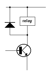
What is the purpose of a diode next to relay on schematics?
Answers & follow ups
- Design a combinational circuit, that multiplies an input
decimal digit represented in BCD by 5. The output is to be
represented in BCD. Show that the outputs can be obtained
from the input lines without using any logic gates.
-
I got this question on the interview to the company that makes flash memory controllers.
They let me take it home and think for a few days. A.M.
There is a system with 4 flash memory banks. When data comes to the system, it will be randomly sent to one of the 4 banks. The system has a feature called Native Command Queuing (NCQ) which allows the host to send multiple commands at a time.
The number of commands sent at a time is called the queue depth. With a queue depth of 1, only 1 of 4 memory banks will be active.
With a queue depth of 2, we expect 2 of 4 flash memory banks to be active except in the case when both commands are to the same bank.
The question is, what is the expected number of flash memory banks that would be active, given queue depths of:
2, 4, 8, and 16 ?Answers & follow ups
Verilog Code for FSMs
Verilog code for an FSM with a single
process.
 module fsm (clk, reset, x1, outp);
 input        clk, reset, x1;
 output       outp;
 reg          outp;
 reg    [1:0] state;
 parameter s1 = 2’b00; parameter s2 = 2’b01;
 parameter s3 = 2’b10; parameter s4 = 2’b11;
 always @(posedge clk or posedge reset)
 begin
    if (reset) begin
       state <= s1; outp <= 1’b1;
    end
    else begin
       case (state)
   s1: begin
   if (x1 == 1’b1) begin
      state <= s2;
                           outp  <= 1’b1;
   end
   else begin
      state <= s3;
                           outp  <= 1’b1;
   end
       end
   s2: begin
   state <= s4;
                        outp  <= 1’b0;
       end
   s3: begin
   state <= s4;
                        outp  <= 1’b0;
       end
   s4: begin
   state <= s1;
                        outp  <= 1’b1;
       end
       endcase
    end
 end
        endmodule
Verilog code for an FSM with two
processes.
 module fsm (clk, reset, x1, outp);
 input        clk, reset, x1;
 output       outp;
 reg          outp;
 reg    [1:0] state;
 parameter s1 = 2’b00; parameter s2 = 2’b01;
 parameter s3 = 2’b10; parameter s4 = 2’b11;
 always @(posedge clk or posedge reset)
 begin
    if (reset)
       state <= s1;
    else begin
       case (state)
   s1: if (x1 == 1’b1)
   state <= s2;
       else
   state <= s3;
   s2: state <= s4;
   s3: state <= s4;
   s4: state <= s1;
       endcase
    end
 end
 always @(state) begin
    case (state)
       s1: outp = 1’b1;
       s2: outp = 1’b1;
       s3: outp = 1’b0;
       s4: outp = 1’b0;
    endcase
 end
        endmodule
Verilog code for an FSM with three
processes.
 module fsm (clk, reset, x1, outp);
 input        clk, reset, x1;
 output       outp;
 reg          outp;
 reg    [1:0] state;
 reg    [1:0] next_state;
 parameter s1 = 2’b00; parameter s2 = 2’b01;
 parameter s3 = 2’b10; parameter s4 = 2’b11;
 always @(posedge clk or posedge reset)
 begin
    if (reset)
       state <= s1;
    else
       state <= next_state;
 end

 always @(state or x1)
 begin
    case (state)
       s1: if (x1 == 1’b1)
       next_state = s2;
    else
       next_state = s3;
       s2: next_state = s4;
       s3: next_state = s4;
       s4: next_state = s1;
    endcase
        end
Verilog Code for RAM & ROM
Verilog code for single-port RAM in read-first
mode.
 module raminfr (clk, en, we, addr, di, do);
 input        clk;
 input        we;
 input        en;
 input  [4:0] addr;
 input  [3:0] di;
 output [3:0] do;
 reg    [3:0] RAM [31:0];
 reg    [3:0] do;
 always @(posedge clk)
 begin
    if (en) begin
       if (we)
   RAM[addr] <= di;

              do <= RAM[addr];
    end
 end
        endmodule
verilog code for a single-port RAM in write-first
mode.
 module raminfr (clk, we, en, addr, di, do);
 input        clk;
 input        we;
 input        en;
 input  [4:0] addr;
 input  [3:0] di;
 output [3:0] do;
 reg    [3:0] RAM [31:0];
 reg    [4:0] read_addr;
 always @(posedge clk)
 begin
    if (en) begin
       if (we)
   RAM[addr] <= di;
              read_addr <= addr;
    end
 end
    assign do = RAM[read_addr];
        endmodule
verilog code for single-port RAM in no-change
mode.
 module raminfr (clk, we, en, addr, di, do);
 input        clk;
 input        we;
 input        en;
 input  [4:0] addr;
 input  [3:0] di;
 output [3:0] do;
 reg    [3:0] RAM [31:0];
 reg    [3:0] do;
 always @(posedge clk)
 begin
    if (en) begin
       if (we)
   RAM[addr] <= di;
       else
   do <= RAM[addr];
    end
 end
        endmodule
Verilog code for a single-port RAM with
asynchronous read.
        module raminfr (clk, we, a, di, do);
        input        clk;
        input        we;
        input  [4:0] a;
        input  [3:0] di;
        output [3:0] do;
        reg    [3:0] ram [31:0];
        always @(posedge clk)
        begin
    if (we)
              ram[a] <= di;
        end
           assign do = ram[a];
        endmodule
Verilog code for a single-port RAM with
"false" synchronous read.
 module raminfr (clk, we, a, di, do);
 input        clk;
 input        we;
 input  [4:0] a;
 input  [3:0] di;
 output [3:0] do;
 reg    [3:0] ram [31:0];
 reg    [3:0] do;
 always @(posedge clk)
 begin
    if (we)
       ram[a] <= di;
    do <= ram[a];
 end
        endmodule
Verilog code for a single-port RAM with
synchronous read (read through).
 module raminfr (clk, we, a, di, do);
 input        clk;
 input        we;
 input  [4:0] a;
 input  [3:0] di;
 output [3:0] do;
 reg    [3:0] ram [31:0];
 reg    [4:0] read_a;
 always @(posedge clk)
 begin
    if (we)
       ram[a] <= di;
    read_a <= a;
 end
    assign do = ram[read_a];
        endmodule
Verilog code for a single-port block RAM
with enable.
        module raminfr (clk, en, we, a, di, do);
        input        clk;
        input        en;
        input        we;
        input  [4:0] a;
        input  [3:0] di;
        output [3:0] do;
        reg    [3:0] ram [31:0];
        reg    [4:0] read_a;
        always @(posedge clk)
        begin
           if (en) begin
              if (we)
                 ram[a] <= di;
              read_a <= a;
           end
        end
           assign do = ram[read_a];
        endmodule
Verilog code for a dual-port RAM with
asynchronous read.
 module raminfr (clk, we, a, dpra, di, spo, dpo);
 input        clk;
 input        we;
 input  [4:0] a;
 input  [4:0] dpra;
 input  [3:0] di;
 output [3:0] spo;
 output [3:0] dpo;
 reg    [3:0] ram [31:0];
 always @(posedge clk)
 begin
    if (we)
       ram[a] <= di;
 end
    assign spo = ram[a];
    assign dpo = ram[dpra];
        endmodule
Verilog code for a dual-port RAM with
false synchronous read.
        module raminfr (clk, we, a, dpra, di, spo, dpo);
        input        clk;
        input        we;
        input  [4:0] a;
        input  [4:0] dpra;
        input  [3:0] di;
        output [3:0] spo;
        output [3:0] dpo;
        reg    [3:0] ram [31:0];
        reg    [3:0] spo;
        reg    [3:0] dpo;
 always @(posedge clk)
        begin
           if (we)
              ram[a] <= di;

           spo = ram[a];
           dpo = ram[dpra];
        end
        endmodule
Verilog code for a dual-port RAM with
synchronous read (read through).
 module raminfr (clk, we, a, dpra, di, spo, dpo);
 input        clk;
 input        we;
 input  [4:0] a;
 input  [4:0] dpra;
 input  [3:0] di;
 output [3:0] spo;
 output [3:0] dpo;
 reg    [3:0] ram [31:0];
 reg    [4:0] read_a;
 reg    [4:0] read_dpra;
 always @(posedge clk)
 begin
    if (we)
       ram[a] <= di;
    read_a <= a;
    read_dpra <= dpra;
 end
    assign spo = ram[read_a];
    assign dpo = ram[read_dpra];
        endmodule
Verilog code for a dual-port RAM with
enable on each port.
 module raminfr (clk, ena, enb, wea, addra, addrb, dia, doa, dob);
 input        clk, ena, enb, wea;
 input  [4:0] addra, addrb;
 input  [3:0] dia;
 output [3:0] doa, dob;
 reg    [3:0] ram [31:0];
 reg    [4:0] read_addra, read_addrb;
 always @(posedge clk)
 begin
    if (ena) begin
       if (wea) begin
   ram[addra] <= dia;
       end
    end
 end

 always @(posedge clk)
 begin
    if (enb) begin
       read_addrb <= addrb;
    end
 end
    assign doa = ram[read_addra];
    assign dob = ram[read_addrb];
        endmodule
Verilog code for a ROM with registered
output.
        module rominfr (clk, en, addr, data);
        input       clk;
        input       en;
        input [4:0] addr;
        output reg [3:0] data;
 always @(posedge clk)
        begin
           if (en)
              case(addr)
                 4’b0000: data <= 4’b0010;
                 4’b0001: data <= 4’b0010;
                 4’b0010: data <= 4’b1110;
                 4’b0011: data <= 4’b0010;
                 4’b0100: data <= 4’b0100;
                 4’b0101: data <= 4’b1010;
                 4’b0110: data <= 4’b1100;
                 4’b0111: data <= 4’b0000;
                 4’b1000: data <= 4’b1010;
                 4’b1001: data <= 4’b0010;
                 4’b1010: data <= 4’b1110;
                 4’b1011: data <= 4’b0010;
                 4’b1100: data <= 4’b0100;
                 4’b1101: data <= 4’b1010;
                 4’b1110: data <= 4’b1100;
                 4’b1111: data <= 4’b0000;
                 default: data <= 4’bXXXX;
              endcase
        end
        endmodule
Verilog code for a ROM with registered
address.
 module rominfr (clk, en, addr, data);
 input       clk;
 input       en;
 input [4:0] addr;
 output reg [3:0] data;
 reg   [4:0] raddr;
 always @(posedge clk)
 begin
    if (en)
       raddr <= addr;
 end

 always @(raddr)
 begin
    if (en)
       case(raddr)
   4’b0000: data = 4’b0010;
   4’b0001: data = 4’b0010;
   4’b0010: data = 4’b1110;
   4’b0011: data = 4’b0010;
   4’b0100: data = 4’b0100;
   4’b0101: data = 4’b1010;
   4’b0110: data = 4’b1100;
   4’b0111: data = 4’b0000;
   4’b1000: data = 4’b1010;
   4’b1001: data = 4’b0010;
   4’b1010: data = 4’b1110;
   4’b1011: data = 4’b0010;
   4’b1100: data = 4’b0100;
   4’b1101: data = 4’b1010;
   4’b1110: data = 4’b1100;
   4’b1111: data = 4’b0000;
   default: data = 4’bXXXX;
       endcase
 end
        endmodule
Verilog code for adders/subtractors
Following is the Verilog code for an unsigned 8-bit adder
with carry in.
 module adder(a, b, ci, sum);
 input  [7:0] a;
 input  [7:0] b;
 input        ci;
 output [7:0] sum;

    assign sum = a + b + ci;

        endmodule
Verilog code for an
unsigned 8-bit adder with carry out.
 module adder(a, b, sum, co);
 input  [7:0] a;
 input  [7:0] b;
 output [7:0] sum;
 output       co;
 wire   [8:0] tmp;

    assign tmp = a + b;
    assign sum = tmp [7:0];
    assign co  = tmp [8];

        endmodule
Verilog code for an unsigned 8-bit adder
with carry in and carry out.
        module adder(a, b, ci, sum, co);
        input        ci;
        input  [7:0] a;
        input  [7:0] b;
        output [7:0] sum;
        output       co;
        wire   [8:0] tmp;

           assign tmp = a + b + ci;
           assign sum = tmp [7:0];
           assign co  = tmp [8];

        endmodule
Verilog code for an unsigned 8-bit
adder/subtractor.
 module addsub(a, b, oper, res);
 input        oper;
 input  [7:0] a;
 input  [7:0] b;
 output [7:0] res;
 reg    [7:0] res;
 always @(a or b or oper)
 begin
    if (oper == 1’b0)
       res = a + b;
    else
       res = a - b;
        end
        endmodule
Verilog code for different MUX
Verilog code for a 4-to-1 1-bit MUX using
an If statement.
 module mux (a, b, c, d, s, o);
 input        a,b,c,d;
 input  [1:0] s;
 output       o;
 reg          o;
 always @(a or b or c or d or s)
 begin
    if (s == 2’b00)
       o = a;
    else if (s == 2’b01)
       o = b;
    else if (s == 2’b10)
       o = c;
    else
       o = d;
 end
        endmodule
Verilog Code for a 4-to-1 1-bit MUX using
a Case statement.
 module mux (a, b, c, d, s, o);
 input        a, b, c, d;
 input  [1:0] s;
 output       o;
 reg          o;
 always @(a or b or c or d or s)
 begin
    case (s)
       2’b00   : o = a;
       2’b01   : o = b;
       2’b10   : o = c;
       default : o = d;
    endcase
 end
        endmodule
Verilog code for a 3-to-1 1-bit MUX with
a 1-bit latch.
        module mux (a, b, c, d, s, o);
        input        a, b, c, d;
        input  [1:0] s;
        output       o;
        reg          o;
        always @(a or b or c or d or s)
        begin
           if (s == 2’b00)
              o = a;
           else if (s == 2’b01)
              o = b;
           else if (s == 2’b10)
              o = c;
        end
        endmodule
Verilog codes for different Shift-registers
Verilog code for an 8-bit shift-left
register with a positive-edge clock, serial in and serial out.
 module shift (clk, si, so);
 input        clk,si;
 output       so;
 reg    [7:0] tmp;
 always @(posedge clk)
 begin
    tmp    <= tmp << 1;
    tmp[0] <= si;
 end
    assign so = tmp[7];
        endmodule
Verilog code for an 8-bit shift-left
register with a negative-edge clock, a clock enable, a serial in and a
serial out.
 module shift (clk, ce, si, so);
 input        clk, si, ce;
 output       so;
 reg    [7:0] tmp;
 always @(negedge clk)
 begin
    if (ce) begin
       tmp    <= tmp << 1;
       tmp[0] <= si;
    end
 end
    assign so = tmp[7];
        endmodule
Verilog code for an 8-bit shift-left
register with a positive-edge clock, asynchronous clear, serial in and
serial out.
 module shift (clk, clr, si, so);
 input        clk, si, clr;
 output       so;
 reg    [7:0] tmp;
 always @(posedge clk or posedge clr)
 begin
    if (clr)
       tmp <= 8’b00000000;
    else
       tmp <= {tmp[6:0], si};
 end
    assign so = tmp[7];
        endmodule
Verilog code for an 8-bit shift-left
register with a positive-edge clock, a synchronous set, a serial in and
a serial out.
 module shift (clk, s, si, so);
 input        clk, si, s;
 output       so;
 reg    [7:0] tmp;
 always @(posedge clk)
 begin
    if (s)
       tmp <= 8’b11111111;
    else
       tmp <= {tmp[6:0], si};
 end
    assign so = tmp[7];
        endmodule
Verilog code for an 8-bit shift-left
register with a positive-edge clock, a serial in and a parallel out.
        module shift (clk, si, po);
        input        clk, si;
        output [7:0] po;
        reg    [7:0] tmp;
        always @(posedge clk)
        begin
           tmp <= {tmp[6:0], si};
        end
           assign po = tmp;
        endmodule
Verilog code for an 8-bit shift-left
register with a positive-edge clock, an asynchronous parallel load, a
serial in and a serial out.
 module shift (clk, load, si, d, so);
 input        clk, si, load;
 input  [7:0] d;
 output       so;
 reg    [7:0] tmp;
 always @(posedge clk or posedge load)
 begin
    if (load)
              tmp <= d;
    else
       tmp <= {tmp[6:0], si};
 end
    assign so = tmp[7];
        endmodule
Verilog code for an 8-bit shift-left
register with a positive-edge clock, a synchronous parallel load, a
serial in and a serial out.
        module shift (clk, sload, si, d, so);
        input        clk, si, sload;
        input  [7:0] d;
        output       so;
        reg    [7:0] tmp;
        always @(posedge clk)
        begin
           if (sload)
              tmp <= d;
           else
              tmp <= {tmp[6:0], si};
        end
           assign so = tmp[7];
        endmodule
Verilog code for an 8-bit
shift-left/shift-right register with a positive-edge clock, a serial in
and a serial out.
 module shift (clk, si, left_right, po);
 input        clk, si, left_right;
 output       po;
 reg    [7:0] tmp;
 always @(posedge clk)
 begin
    if (left_right == 1’b0)
       tmp <= {tmp[6:0], si};
    else
       tmp <= {si, tmp[7:1]};
 end
    assign po = tmp;
        endmodule
verilog code for ACCUMULATOR
Verilog code for a 4-bit unsigned up
accumulator with an asynchronous clear.
        module accum (clk, clr, d, q);
        input        clk, clr;
        input  [3:0] d;
        output [3:0] q;
        reg    [3:0] tmp;
        always @(posedge clk or posedge clr)
        begin
           if (clr)
              tmp <= 4’b0000;
           else
              tmp <= tmp + d;
        end
           assign q = tmp;
        endmodule
Verilog Codes for different COUNTERS
Verilog code for a 4-bit unsigned up
counter with asynchronous clear.
        module counter (clk, clr, q);
        input        clk, clr;
        output [3:0] q;
        reg    [3:0] tmp;
        always @(posedge clk or posedge clr)
        begin
           if (clr)
              tmp <= 4’b0000;
           else
              tmp <= tmp + 1’b1;
        end
           assign q = tmp;
        endmodule
Verilog code for a 4-bit unsigned down
counter with synchronous set.
        module counter (clk, s, q);
        input        clk, s;
        output [3:0] q;
        reg    [3:0] tmp;
        always @(posedge clk)
        begin
           if (s)
              tmp <= 4’b1111;
           else
              tmp <= tmp - 1’b1;
        end
           assign q = tmp;
        endmodule
Verilog code for a 4-bit unsigned up
counter with an asynchronous load from the primary input.
        module counter (clk, load, d, q);
        input        clk, load;
        input  [3:0] d;
        output [3:0] q;
        reg    [3:0] tmp;
        always @(posedge clk or posedge load)
        begin
           if (load)
              tmp <= d;
           else
              tmp <= tmp + 1’b1;
        end
           assign q = tmp;
        endmodule
Verilog code for a 4-bit unsigned up
counter with a synchronous load with a constant.
 module counter (clk, sload, q);
 input        clk, sload;
 output [3:0] q;
 reg    [3:0] tmp;
 always @(posedge clk)
 begin
    if (sload)
              tmp <= 4’b1010;
    else
       tmp <= tmp + 1’b1;
 end
    assign q = tmp;
        endmodule
Verilog code for a 4-bit unsigned up
counter with an asynchronous clear and a clock enable.
 module counter (clk, clr, ce, q);
 input        clk, clr, ce;
 output [3:0] q;
 reg    [3:0] tmp;
 always @(posedge clk or posedge clr)
 begin
    if (clr)
       tmp <= 4’b0000;
    else if (ce)
       tmp <= tmp + 1’b1;
 end
    assign q = tmp;
        endmodule
Verilog code for a 4-bit unsigned up/down
counter with an asynchronous clear.
 module counter (clk, clr, up_down, q);
 input        clk, clr, up_down;
 output [3:0] q;
 reg    [3:0] tmp;
 always @(posedge clk or posedge clr)
 begin
    if (clr)
       tmp <= 4’b0000;
    else if (up_down)
       tmp <= tmp + 1’b1;
    else
       tmp <= tmp - 1’b1;
 end
    assign q = tmp;
        endmodule
e Verilog code for a 4-bit signed up
counter with an asynchronous reset.
        module counter (clk, clr, q);
        input               clk, clr;
        output signed [3:0] q;
        reg    signed [3:0] tmp;
        always @ (posedge clk or posedge clr)
        begin
           if (clr)
              tmp <= 4’b0000;
           else
              tmp <= tmp + 1’b1;
        end
           assign q = tmp;
        endmodule
Verilog code for a 4-bit signed up
counter with an asynchronous reset and a modulo maximum.
        module counter (clk, clr, q);
        parameter MAX_SQRT = 4, MAX = (MAX_SQRT*MAX_SQRT);
        input                 clk, clr;
        output [MAX_SQRT-1:0] q;
        reg    [MAX_SQRT-1:0] cnt;
        always @ (posedge clk or posedge clr)
        begin
           if (clr)
              cnt <= 0;
           else
              cnt <= (cnt + 1) %MAX;
        end
           assign q = cnt;
        endmodule
Subscribe to:
Posts (Atom)